Talk about the design experience of switching power supply for many years, from switching power supply PCB design, PCB layout, PCB copper trace, aluminum substrate and multilayer PCB in switching power supply, to flyback power supply Duty cycle, the absolute essence of practice!
Switch Power Supply PCB Design
First of all, from the switching power supply design and production process to describe it, first talk about the design of the printed board. Switching power supply operates at high frequency and high pulse state and belongs to a special kind of analog circuit. When laying out the board must follow the principle of high-frequency circuit wiring.
Layout: The pulse voltage connection is as short as possible, in which the input switch tube is connected to the transformer, and the output transformer is connected to the rectifier tube connection wire. The pulse current loop is as small as possible if the input filter capacitor is going to the transformer and the return capacitance of the switch tube is negative. Output part of the transformer's output terminal to the rectifier to the output capacitor to the output capacitor returns to the transformer circuit. The X capacitor should be as close as possible to the switching power supply input. The input line should be avoided parallel to other circuits and should be avoided. The Y capacitor should be placed on the chassis ground terminal or FG connector. The common touch sensor keeps a certain distance from the transformer to avoid magnetic coupling. If it is difficult to handle, a shield can be added between the common touch inductor and the transformer. The above items have a greater impact on the EMC performance of the switching power supply.
The output capacitor can generally be two near one rectifier tube and the other should be close to the output terminal, which can affect the power output ripple index. The effect of two small-capacity capacitors in parallel should be better than using a large-capacity capacitor. Heating devices and electrolytic capacitors to maintain a certain distance, in order to extend the life of the whole machine, electrolytic capacitors is the life of the switch power supply bottle, such as transformers, power tubes, high power resistors and electrolysis to keep the distance between the electrolysis must also leave room for heat , conditions allow it can be placed in the air inlet.
The control part should pay attention to: high-impedance weak signal circuit connection should be as short as sampling feedback loop, to avoid interference when it is processed, the current sampling signal circuit, especially the current control circuit, processing is not easy and some unexpected Unexpectedly.
Let's talk about some principles of PCB layout.
Line spacing: With the continuous improvement and improvement of the manufacturing process of the printed circuit board, it is no longer a problem that the average line spacing of the manufacturing plant is equal to or less than 0.1 mm, and it can fully satisfy most applications. Taking into account the components and production technology used in the switching power supply, the minimum double-panel spacing is generally set to 0.3mm, the minimum single-panel spacing is set to 0.5mm, and the pads and pads, pads and vias or vias The minimum distance between holes is set to 0.5mm to avoid “bridging†during the welding operation. This allows most board manufacturers to easily meet production requirements, and can control the finished product rate very high and can also achieve reasonable results. The wiring density and there is a more economical cost.
The minimum line spacing is only suitable for signal control circuits and low voltage circuits with voltages lower than 63V. When the line voltage is greater than this value, the line spacing can generally be taken in accordance with the 500V/1mm empirical value.
In view of the fact that some relevant standards have more specific provisions for line spacing, they must be implemented in strict accordance with standards, such as the AC inlet to the fuse-end connection. Some power supplies require high volume, such as module power. It is practically proven that the transformer side input line spacing is 1mm. For AC input, (isolated) DC output power supply products, the more stringent requirement is that the safety clearance should be greater than or equal to 6mm, which of course is determined by the relevant standards and implementation methods. The general safety distance can be referenced by the distance between the two ends of the feedback optocoupler. The principle is greater than or equal to this distance. It is also possible to slot the printed board under the optocoupler to increase the creepage distance to meet the insulation requirements. Generally, the spacing between the AC input side of the switching power supply or the board components should be more than 5mm away from the non-insulated housing and the heat sink, and the distance between the output side wiring or the components from the housing or the heat sink should be greater than 2mm, or strictly in accordance with the safety regulations.
Commonly used methods: The circuit board grooving method mentioned above is suitable for some occasions with insufficient spacing. By the way, this method is also commonly used as a protective discharge gap, which is common in the TV display tube and power supply AC input. . This method has been widely used in the module power supply, and it can obtain good results under the conditions of potting.
Method 2: Pad insulation paper, green shell paper, polyester film, PTFE oriented film and other insulating materials. The general purpose power supply is covered with green shell paper or polyester film on the circuit board between the metal chassis. This material has high mechanical strength and certain resistance to moisture. Due to its high temperature resistance, PTFE orientation films are widely used in module power supplies. An insulating film can also be placed between the component and the surrounding conductors to increase the insulation resistance.
Note: Some device insulation covers may not be used as insulating media to reduce safety clearances, such as electrolytic capacitor skins, which may heat shrink under high temperature conditions. A space is reserved for the front end of the large-scale electrolytic explosion-proof tank to ensure that the electrolytic capacitor can be evacuated without hindrance under extreme conditions.
PCB copper traces considerations
Trace Current Density: Most electronic circuits now consist of insulating copper. The thickness of commonly-used PCB copper foil is 35μm, and the current density can be taken from the trace value of 1A/mm. The specific calculation can be found in textbooks. In order to ensure the mechanical strength of the wiring, the line width should be greater than or equal to 0.3mm (other non-power circuit boards may have a smaller minimum line width). Copper board thickness of 70μm circuit board is also common in switching power supply, then the current density can be higher.
To add that, the commonly used circuit board design tool software generally has design specifications, such as line width, line spacing, and the size of the dry hole through hole can be set. When designing a circuit board, the design software can be automatically executed according to the specifications, which can save a lot of time, reduce part of the workload, and reduce the error rate.
In general, high-reliability lines or wiring lines with high density can be double-sided. Its characteristics are moderate cost, high reliability, and can meet most applications.
The module power supply ranks some products to use the multi-layer board, mainly is advantageous for integrating the transformer inductance and so on power device, optimizes the wiring, the power tube heat dissipation and so on. It has the advantages of good craftsmanship, good consistency and good heat dissipation of the transformer, but its disadvantages are high cost and poor flexibility, and it is only suitable for industrial large-scale production.
Single-panel, market-oriented general-purpose switching power supply uses almost single-sided circuit board, which has the advantages of low cost, and some measures can be taken to ensure its performance in design and production processes.
Talk about some experience of single-sided PCB design
Because the single panel has the characteristics of low cost and easy manufacture, it is widely used in switching power supply circuits. Since it has only one side of copper, the electrical connection of the device and the mechanical fixing rely on that layer of copper skin, care must be taken when handling it.
In order to ensure a good welding mechanical structure performance, the single-sided pad should be slightly larger to ensure a good bonding force between the copper skin and the substrate, without the copper skin peeling off and breaking when shocked. The general weld ring width should be greater than 0.3mm. The diameter of the pad hole should be slightly larger than the diameter of the device pin, but should not be too large, to ensure the shortest distance between the pin and the pad by the solder, the size of the hole is not to hinder the normal check for the degree, the pad hole diameter is generally greater than the pin Diameter 0.1-0.2mm. Multi-pin devices can also be larger to ensure a smooth inspection.
The electrical connection should be as wide as possible, and the principle width should be greater than the pad diameter. In special cases, the line must be widened (commonly known as teardrop generation) when connecting to the pad. This prevents the wire from breaking under certain conditions. The principle minimum line width should be greater than 0.5mm.
Components on a single panel should be close to the circuit board. Devices that require overhead heat dissipation must be sleeved on the pins between the device and the circuit board, which can play the dual role of supporting the device and increasing insulation. To minimize or avoid the impact of external forces on the pad and the pin joint The resulting impact enhances the firmness of the weld. The components with larger weight on the circuit board can increase the supporting connection points, and can strengthen the connection strength with the circuit board, such as transformers and power device radiators.
The single-sided soldered surface leads can be left longer without affecting the space between the shells. The advantage is that the strength of the solder joint can be increased, the soldering area can be increased, and the solder joint can be found instantly. Longer leg shears have less stress on the weld area. In Taiwan and Japan, it is common practice to bend the device pins at the solder surface to form a 45-degree angle with the circuit board, and then solder the process. Today, we talked about some matters in the double-panel design. In some application environments where the requirements are relatively high, or where the wiring density is relatively large, the use of double-sided printed boards has much better performance and indicators than that of single-sided boards.
Due to the high metallurgical strength of the hole in the dual-panel pad, the solder ring can be smaller than the single-sided pad. The hole diameter of the pad hole can be slightly larger than the diameter of the pin because the solder solution penetrates the top layer through the hole in the soldering process. Pads to increase soldering reliability. However, there is a drawback that if the hole is too large, part of the device may float under the jet tin impact during wave soldering, resulting in some defects.
For the processing of large-current traces, the line width can be processed according to the previous post. If the width is not enough, the thickness can be increased by adding tin on the traces. The methods are various.
1. Set the trace as a pad attribute so that the trace will not be covered by the solder mask during the manufacture of the circuit board. Hot air will be plated with tin when leveled.
2, place the pad at the wiring place, set this pad to the shape that needs to route, pay attention to set the pad hole to zero.
3, Place the wire in the solder mask, this method is the most flexible, but not all circuit board manufacturers will understand your intentions, need to use text instructions. Solder is not applied where the solder mask is placed.
Several methods of tinning of the circuit are as above. It should be noted that if a very wide trace is plated with tin, after soldering, a large amount of solder will be adhered, and the distribution is very uneven, affecting the appearance. Slim strips are generally used. The width of tin plating is 1~1.5mm. The length can be determined according to the circuit. The tinned part is separated by 0.5~1mm. The double-sided circuit board provides great selectivity for layout and routing, and can make the wiring more Tends to be reasonable. Regarding grounding, the power ground must be separated from the signal ground, and the two grounds can be connected at the filter capacitor to avoid the unpredictable and unpredictable factors caused by the connection of large pulse currents through the signal ground. The signal control loop should adopt a one-point grounding method as far as possible. There is a technique to place ungrounded traces on the same wiring layer as much as possible, and finally on the other floor. The output line is generally passed through the filter capacitor, and then to the load. The input line must also pass through the capacitor and then to the transformer. The theoretical basis is to let the ripple current pass through the brigade filter capacitor.
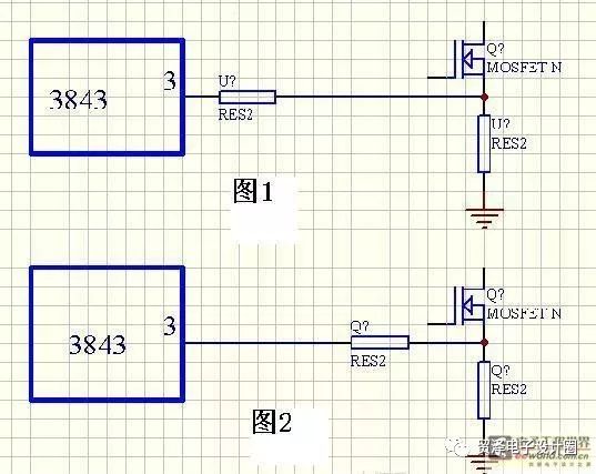
Voltage feedback sampling, in order to avoid the impact of large current through the trace, the sampling point of the feedback voltage must be placed on the most power output end, in order to improve the overall load effect index.
The change of the wiring from one wiring layer to another is generally via-hole communication. It is not suitable to realize the pin pad of the device because the connection relationship may be destroyed during the insertion of the device, and the current per 1A is passed. There should be at least 2 vias, the via hole diameter principle should be greater than 0.5mm, generally 0.8mm can ensure the processing reliability.
The device can dissipate heat. In some low-power power supplies, the circuit board traces can also function as heat sinks. The feature is that the traces are as wide as possible to increase the heat dissipation area, and no solder resist is applied. The vias can be evenly placed to enhance the thermal conductivity. .
Application of Aluminum Substrates and Multilayer Printed Boards in Switching Power Supply
Then talk about the application of aluminum substrates in switching power supplies and the application of multilayer printed boards in switching power supply circuits.
The aluminum substrate is constructed by itself and has the following characteristics: the thermal conductivity is very good, the copper is bonded on one side, the device can only be placed on the copper bonding surface, and the electrical connection hole cannot be opened so that the jumper cannot be placed as a single panel.
The aluminum substrate is generally placed on a chip device, a switch tube, and an output rectifier tube conducts heat through the substrate. The thermal resistance is very low and high reliability can be achieved. The transformer adopts the planar patch structure, which can also dissipate heat through the substrate, and its temperature rise is lower than conventional. The transformer of the same size adopts the aluminum substrate structure to obtain a larger output power. Aluminum board jumpers can be bridged. The aluminum substrate power supply is generally composed of two printed boards, and the other board is placed with a control circuit. The two boards are physically integrated and integrated.
Due to the excellent thermal conductivity of the aluminum substrate, it is difficult to weld in a small amount by hand, the solder is cooled too quickly, and the problem is easily arisen. A simple and practical method is available. One ordinary ironing iron (preferably having a thermostat function) is used. Turn over, press the iron up, fix it, fix the temperature, adjust the temperature to about 150°C, put the aluminum plate on the iron, warm it for a while, then stick and weld the components according to the conventional method. The iron temperature is suitable for easy soldering of the device. If the device is too high, the device may be damaged, and even the copper plate of the aluminum substrate may peel off. The temperature is too low and the welding effect is not good.
In recent years, with the application of multi-layer circuit boards in switching power supply circuits, printed circuit transformers have become possible. Due to the multi-layered boards and the small layer spacing, transformer window cross-sections can also be fully utilized and can be used on the main circuit board. Add one to two printed coils composed of multi-layer boards to achieve the purpose of using the window to reduce the current density of the circuit. Due to the use of printed coils, manual intervention is reduced, the transformer has good consistency, the planar structure, low leakage inductance, and good coupling. . Open magnetic core, good heat dissipation conditions. Because it has many advantages and is conducive to mass production, it has been widely used. However, the initial investment in research and development is relatively large and it is not suitable for small-scale students.
Switching power supply is divided into two types: isolation and non-isolation. Here, the topology of the isolated switching power supply is mainly discussed. In the following, unless otherwise specified, all refer to isolated power supply. The isolated power supplies can be divided into two major categories according to their structural types: forward and flyback. Flyback means that when the primary side of the transformer turns on, the secondary side ends and the transformer stores energy. When the primary side is cut off, the secondary side is turned on and the energy is released to the working state of the load. Generally, the conventional flyback power supply has many single and multiple tubes, and the two tubes are not common. Forward mode means that the primary side of the transformer is conducting while the secondary side induces a corresponding voltage output to the load, and energy is directly transmitted through the transformer. According to the specifications can be divided into conventional forward, including single forward, double forward. Half-bridge and bridge circuits are forward circuits.
The forward and flyback circuits each have their own characteristics. In the process of designing the circuit, it can be used flexibly to achieve the optimal price/performance ratio. The flyback type is generally available in low power applications. Slightly larger can use single-switch forward circuit, medium power can use double-switch forward circuit or half-bridge circuit, low-voltage push-pull circuit, and half-bridge work the same state. High power output generally uses a bridge circuit, and low voltage can also adopt a push-pull circuit.
Because of its simple structure, the flyback power supply eliminates an inductor that is approximately the same size as the transformer and is widely used in small and medium power supplies. In some of the introductions, the power of the flyback power supply can only be tens of watts, and there is no advantage in output power exceeding 100 watts, making it difficult to implement. I think this is the case in general, but it cannot be said that PI's TOP chip can achieve 300 watts. Some articles describe that the flyback power supply can achieve a kilowatt, but no physical object has been seen. The output power is related to the output voltage.
The leakage inductance of the flyback power transformer is a very critical parameter. Since the flyback power supply requires the transformer to store energy, in order to make full use of the transformer core, it is generally necessary to open an air gap in the magnetic circuit. Its purpose is to change the core hysteresis. The slope of the loop allows the transformer to withstand large pulsed current surges without the core entering a saturated, non-linear state. The air gap in the magnetic circuit is in a high reluctance state. The magnetic leakage in the magnetic circuit is much larger than in the fully closed magnetic circuit. .
The coupling between the primary poles of the transformer is also a key factor in determining the leakage inductance. The primary coils should be as close as possible and sandwich winding can be used, but this will increase the distributed capacitance of the transformer. Use iron core as long as possible to use a longer core of the window, can reduce the leakage inductance, such as using EE, EF, EER, PQ type core effect is better than EI type.
Regarding the duty cycle of the flyback power supply, in principle, the maximum duty cycle of the flyback power supply should be less than 0.5, otherwise the loop is not easy to compensate and may be unstable, but there are some exceptions, such as the TOP series of chips introduced by the US PI company is Can work at duty ratios greater than 0.5. The duty cycle is determined by the ratio of turns of the primary winding of the transformer. I believe that the reflected voltage is determined first (the output voltage is reflected by the transformer and reflected to the primary voltage), and the reflected voltage is increased within a certain voltage range. The duty cycle increases and the switching loss decreases. When the reflected voltage decreases, the duty cycle decreases and the switching loss increases. Of course, this is also a prerequisite, when the duty cycle increases, it means that the output diode conduction time is shortened, in order to maintain the output stability, more time will be guaranteed by the output capacitor discharge current, the output capacitor will withstand greater high frequency Ripple current rushes, causing it to heat up, which is not allowed under many conditions. Increasing the duty cycle and changing the turns ratio of the transformer will increase the leakage inductance of the transformer and make its overall performance change. When the leakage inductance energy is large enough, it can fully offset the low loss caused by the large duty cycle of the switch. At that time, the significance of the duty cycle is not further increased, and the switch may be broken even if the reverse-peak voltage of the leakage inductance is too high. Due to the large leakage inductance, output ripple and other electromagnetic parameters may be degraded. When the duty cycle is small, the switch tube passes the high RMS current value, and the transformer primary current has a large RMS value, which reduces the efficiency of the converter, but it can improve the working conditions of the output capacitor and reduce heat generation. How to determine the transformer reflected voltage (ie, duty cycle).
Some netizens mentioned the setting of the feedback loop of the switching power supply and the analysis of the working status. Due to the poor mathematics at school, the "Automatic Control Principles" almost make up for the exam. Now it still feels fear for this door, and now it can't completely write the closed loop system transfer function. It's a concept of system zero and pole. Very vague, seeing the Bode diagram is only about to see if it is divergence or convergence, so the feedback compensation does not dare to go nuts, but there are some suggestions. If there is some mathematics skills, there will be some study time to find out the textbook “Automatic Control Principle†of the university carefully and combine it with the actual switching power supply circuit to analyze according to the working status.
Flyback power supply duty cycle
Finally talk about the duty cycle of the flyback power supply (I pay attention to the reflected voltage, consistent with the duty cycle), the duty cycle is also related to the pressure of the selected switch, there are some early flyback power supply using a relatively low pressure switch Tubes, such as 600V or 650V as the exchange of 220V input power switch, may be related to the production process at that time, high pressure pipe, not easy to manufacture, or low pressure pipe has more reasonable conduction loss and switching characteristics, like this line The reflected voltage must not be too high. Otherwise, in order to operate the switch in a safe range, the power absorbed by the circuit is also considerable. Practice has proved that 600V tube reflection voltage should not be greater than 100V, 650V tube reflection voltage should not be greater than 120V, when the leakage inductance peak voltage value is clamped at 50V, the tube still has 50V working margin. Now due to the improvement of MOS tube manufacturing technology, the general flyback power supply uses 700V or 750V or even 800-900V switch tubes. Like this kind of circuit, the ability of anti-overvoltage is strong Some switch transformer reflection voltages can also be made higher, the maximum reflection voltage is more suitable at 150V, can obtain better comprehensive performance. PI's TOP chip is recommended to use 135V transient voltage suppression diode clamp. However, the evaluation voltage of his evaluation board is generally lower than this value at about 110V. Both types have their own advantages and disadvantages:
The first type: Disadvantages The anti-overvoltage capability is weak, the duty cycle is small, and the transformer primary pulse current is large. Advantages: Transformer leakage inductance is small, electromagnetic radiation is low, ripple index is high, switching tube loss is small, conversion efficiency is not necessarily lower than the second category.
The second type: The disadvantages of the switch tube are larger, and the leakage inductance of the transformer is larger and the ripple is worse. Advantages: Strong over-voltage resistance, large duty cycle, low transformer losses, high efficiency.
Flyback power supply voltage also has a definite factor. The reflected voltage of the flyback power supply is also related to a parameter, that is, the output voltage. The lower the output voltage is, the larger the transformer turns ratio is. The greater the leakage inductance of the transformer, the higher the leakage voltage of the transformer. The higher the potential for breakdown of the switch tube, the greater the power consumed by the snubber circuit, and the potential for permanent failure of the absorption loop power device (especially with transient suppression diodes). In the process of designing the low-voltage output low-power flyback power supply optimization, it must be handled with care. There are several ways to handle it:
1, the use of a large power level of the core to reduce the leakage inductance, which can improve the conversion efficiency of low-voltage flyback power supply, reduce losses, reduce output ripple, improve the cross-regulation rate of multi-output power supply, commonly used in home appliances switch Power supplies, such as CD players, DVB set-top boxes, etc.
2. If the condition does not allow the core to be increased, only the reflected voltage can be reduced and the duty cycle can be reduced. Lowering the reflection voltage can reduce the leakage inductance but may reduce the power conversion efficiency. This is a contradiction. There must be an alternative process to find a suitable point. During the transformer replacement experiment, the primary side of the transformer can be detected. The peak-to-peak voltage minimizes the width and amplitude of the peak-to-peak voltage pulses and increases the operating margin of the converter. The general reflection voltage is more appropriate at 110V.
3, enhance the coupling, reduce losses, using new technology, and winding process, the transformer in order to meet the safety standards will take insulation measures between the primary and secondary sides, such as pad insulation tape, add the end of the empty tape. These will affect the leakage inductance of the transformer. In actual production, the primary winding can be used to wrap around the secondary winding. Or secondary winding with triple insulated wire, eliminating insulation between the primary and secondary, can enhance the coupling, and even a wide copper skin can be used.
The low voltage output in the text refers to an output less than or equal to 5V. Like my low-power power supply, my experience is that a power output greater than 20W can be forward-typed to obtain the best price/performance ratio. Of course, this is not correct. Personal habits, the application of the environment are related, the next time talk about the magnetic core of the flyback power supply, the magnetic circuit to open some of the air gap, I hope that the Supreme urged.
The flyback power transformer core is operating in a unidirectional magnetization state, so the magnetic circuit needs to open an air gap, similar to a pulsating DC inductor. Some magnetic circuits are coupled through air gaps. The principle of opening the air gap is understood as: Since the power ferrite also has an approximately rectangular operating characteristic curve (hysteresis loop), the Y axis represents the magnetic induction intensity (B) on the operating characteristic curve, and the current production process is general. The saturation point is above 400mT. Generally, the value in the design should be 200-300mT, and the X-axis is the magnetic field strength (H). This value is proportional to the strength of the magnetizing current. The open magnetic gap of the magnetic circuit is equivalent to tilting the magnetic hysteresis loop of the magnet toward the X axis. Under the same magnetic induction intensity, it can withstand more magnetization current, which is equivalent to the magnetic core storing more energy. This energy is cut off at the switch. When the transformer secondary diarrhoea is placed into the load circuit, the flyback power core has two roles. One is to transfer more energy and the other to prevent the core from entering saturation.
The transformer of the flyback power supply operates in a unidirectional magnetization state, not only to transfer energy through magnetic coupling, but also to take multiple roles of voltage conversion input and output isolation. Therefore, the air gap must be handled with great care. If the air gap is too large, the leakage inductance will increase, the hysteresis loss will increase, and the iron loss and copper loss will increase, affecting the overall performance of the power supply. A small air gap can saturate the transformer core and cause damage to the power supply.
The continuous and discontinuous mode of the so-called flyback power supply refers to the working state of the transformer. In the fully loaded state, the transformer works in a working mode in which the energy is completely transmitted or incompletely transmitted. Generally, according to the working environment, the conventional flyback power supply should be operated in a continuous mode, so that the loss of switches and lines is relatively small, and the working stress of the input and output capacitors can be reduced, but there are some exceptions.
It needs to be pointed out here: Because the characteristics of flyback power supplies are also more suitable for designing as high voltage power supplies, high voltage power supply transformers generally work in discontinuous mode. I understand that high voltage power supply rectifier diodes are required for high voltage power supply output. Due to the characteristics of the manufacturing process, high back-pressure diodes have long reverse recovery time and low speed. In the continuous current state, the diode recovers when there is forward bias, and the energy loss during reverse recovery is very large, which is not conducive to the performance of the converter. The improvement will reduce the conversion efficiency, and the rectifier tube will be very hot, and even it will burn the rectifier tube. Since in the discontinuous mode, the diode is reverse biased at zero bias, the loss can be reduced to a relatively low level. So the high voltage power supply operates in discontinuous mode, and the operating frequency cannot be too high.
There is also a type of flyback power supply operating in a critical state. Generally, this type of power supply operates in the frequency modulation mode, or in the dual-mode FM widening mode. Some low-cost self-oscillating power supplies (RCCs) often use this type of transformer to ensure stable output. The operating frequency varies with the output current or input voltage, and the transformer is always kept between continuous and intermittent when it is fully loaded. This type of power supply is only suitable for low power output, otherwise the handling of electromagnetic compatibility characteristics can be a headache.
Flyback switching power supply transformers should work in continuous mode, it requires a relatively large winding inductance, of course, there is a certain degree of continuous, excessive pursuit of absolute continuity is unrealistic, may require a large core, very many The number of coil turns, accompanied by a large leakage inductance and distributed capacitance, may not be worth the loss. Then how to determine this parameter, through multiple practices, and analysis of the peer's design, I believe that when the nominal voltage input, the output reaches 50% ~ 60% transformer from intermittent, transition to a continuous state is more appropriate. Or, in the state of the highest input voltage, when the output is full, the transformer can transition to the continuous state.
2835 Led Strip,Single Color Led Strips,Single Color Light,Led Single Light Strip
NINGBO SENTU ART AND CRAFT CO.,LTD. , https://www.lightworld-sentu.com