TOP1 Electronic wallet circuit design based on NFC technology control
NFC has the characteristics of two-way connection and identification, working in the frequency range of 13.56MHz, and the working distance is close to 10 cm. NFC technology promotes standardization under the ISO 18092, ECMA 340 and ETSI TS 102 190 frameworks, and is also compatible with the widely used ISO 14443 Type-A, B and Felica standard contactless smart cards. Compliant with the latest NFC specifications developed by the European Telecommunications Standards Institute (ETSI), the PN544 provides mobile phone manufacturers and telecom operators with a fully compatible platform for the next generation of NFC devices and services: the PN544 is fully compatible with all available single-line Protocol (SWP) The NFC specification for connecting the SIM card to the Host Controller Interface (HCI).
The NFC RF circuit is composed of an EMC filter circuit, a matching circuit, a receiving circuit, and an antenna. Since the system is based on an operating frequency of 13.56 MHz. This frequency is generated by a quartz crystal. At the same time, high-order harmonics are generated. In order to comply with the internal electromagnetic compatibility rules, higher-order harmonics of three, five, and five times of 13.56 MHz must be appropriately suppressed. Therefore, the EMC circuit is configured as an LC low-pass filter for filtering out higher harmonics.
Antenna matching circuit design
Since the antenna coil itself is a low-impedance device, in order to maximize the transfer of energy from the NFC IC to the antenna, a matching circuit must be added between the antenna and the NFC IC. Eliminate the energy loss caused by signal reflection caused by mismatch. The receiving circuit is composed of R127, C118, R128, C119. The Vmid potential generated inside the chip is used as the input potential of the RX pin. To reduce the disturbance, the capacitor should be used to ground Vmid. The bias voltage of Vmid can increase the voltage drive of the Rx pin. Figure 2 shows the NFC RF receiver circuit.
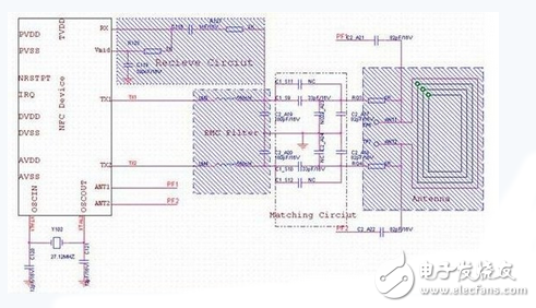
Figure 2 NFC RF part of the circuit
The NXP practical NFC e-wallet solution in this paper is based on the operating frequency of 13.56MHz, using the mobile phone as the trading platform, and the mobile payment and data are realized by the NXP PN544 NFC controller (the built-in security module of PN65O) and the security module. The exchange function provides a convenient, safe and extraordinary experience for electronic payment.
Circuit design based on NFC universal card reader
In many current RFID applications, device manufacturers may not be able to determine which transceivers the customer uses, especially transceiver chips. Therefore, in order to maximize the chances of winning a bid in a particular project, the device manufacturer must provide such a card reader, either it can support as many transceiver chips as possible on the market, or it is at least relatively easy. Customized. In addition to requiring a range of protocols, standards, and transceivers, customers may have other functional requirements for card readers such as high performance, collision avoidance, far/near sensing distance, mobility, and power consumption. But it is difficult to meet so many requirements at the same time in a single card reader. To meet all of these requirements, manufacturers may need to provide a range of readers that can meet different requirements.
The EM4094 is an integrated transceiver chip that can be used to build analog front-end modules for RFID readers. The chip's data transmission and reception links allow the transmission and decoding of any communication protocol, so the EM4094 supports all EM's 13.56MHz transceiver chips, ISO15693, ISO14443 A&B, and Sony Felica protocols. With proper settings, the EM4094 can even communicate with NFC devices. This article will walk through a series of steps to illustrate how a hardware engineer should integrate and utilize the EM4094 RFID reader circuit.
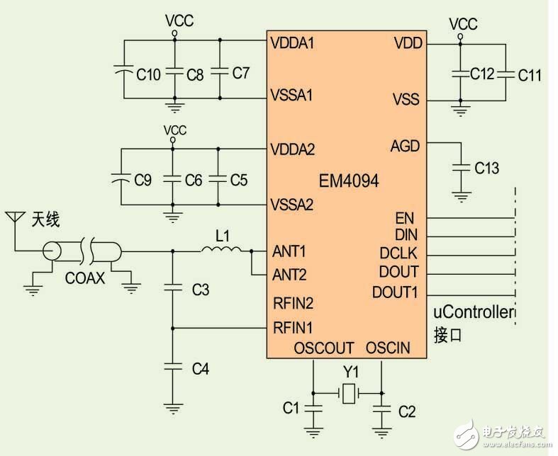
Figure 1: Typical application circuit configuration.
Antenna driver output circuit design
ANT1 and ANT2 are the two outputs of the antenna driver, which can be driven in phase or in phase, which makes it possible to connect the reader antennas in different ways and to generate four antennas of different power levels depending on the chosen configuration. The EM4094 can also be used with a remote antenna where the output impedance of the EM4094 (see Figure 3) must match the impedance of the communication line.
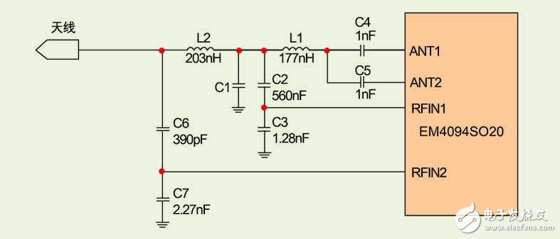
Figure 3: Impedance matching circuit.
If a coaxial cable is used, the output impedance of the EM4094 will have to be adjusted between 10 ohms (ANT1 selectable) and 50 ohms with only one antenna driver; the output of the EM4094 when the two antennas are used in parallel The impedance will have to be adjusted between 5 ohms (ANT1 moveable) and 50 ohms. To achieve a good impedance match, developers can choose to use an LC PI network and select the appropriate component parameter values ​​with the Smith chart.
If the reader antenna can be integrated on the same PCB as the EM4094, you can use the direct antenna connection method (see Figure 2). In this case, the antenna and series capacitor form an LC series loop. The resonant frequency of this loop is the frequency of the reader. The series resistor is used to suppress the quality factor and set the antenna current below the EM4094 rating. When the antenna is operating at its resonant frequency, direct connection to the antenna results in higher power. The different connection methods for IC antennas can be found in the EM4094 Application Guide.
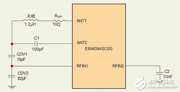
Figure 2: Direct antenna connection.
Transceiver signal reception
RFIN1 and RFIN2 are the two input pins on the IC receive chain. They are used by the EM4094 to demodulate the data stream sent by the transceiver. The voltage on the pin must be set between GND and VDD. The demodulation inputs must have the same performance and exhibit the same sensitivity. In conjunction with an external matched impedance circuit, these two inputs can be used to demodulate the input phase or amplitude modulated signal. Unused input pins should be connected to analog ground through a 10nF capacitor. The high sensitivity of the input pins allows the reader to have a farther read range even at the lowest power level of the electronic tag.
3.5 Mm Audio Jack Panel Mount,3.5 Mm Panel Mount Jack,Audio 3.5 Mm Port,3.5 Mm Aux Port
Dongguan Swan Electronic Technology Co., Ltd , https://www.swanconnector.com